BM1384 is a kind of high-performance and low-power consumption bitcoin mining ASIC for Antminer S5.
1. Feature
• Typical hash rate and power
Voltage(V) | Hash Rate(GH/S) | Current(A) | Total power(W) | W/GH |
0.80 | 22.00 | 12.310 | 9.848 | 0.448 |
0.75 | 17.88 | 9.200 | 6.900 | 0.386 |
0.72 | 15.13 | 7.440 | 5.357 | 0.354 |
0.70 | 13.75 | 6.600 | 4.620 | 0.336 |
0.65 | 11.00 | 4.460 | 2.899 | 0.264 |
0.60 | 8.25 | 3.430 | 2.058 | 0.249 |
• Customized package
• Support UART communication interface
• Support chain mode, Max 256 chips per chain
• Support hardware addressing and software addressing
2. Applications
Bitcoin mining for Antminer S5
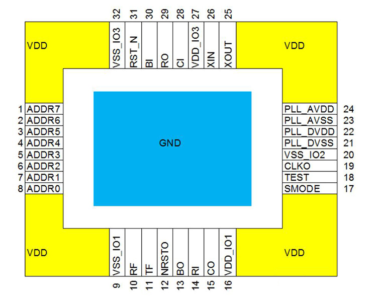
1. Pin diagram

2. Signal Description
Name | I/O | Active Level | Description |
XIN | I | N/A | Oscillator input |
XOUT | O | N/A | Oscillator output |
RST_N | I | L | Reset signal |
TEST | I | N/A | Internal pull down. 0: Normal mode 1: Test mode |
SMODE | I | N/A | Serial Mode. Internal pull up. 0: Asynchronous UART mode. 1: Synchronous UART mode. |
CLKOUT | O | N/A | Clock output |
NRSTO | O | L | Reset output |
CI | I | N/A | Command Input. Schmitt input. |
CO | O | N/A | Command Output |
RI | I | N/A | Respond Input. Schmitt input and internal pullup. |
RO | O | N/A | Respond Output |
BI | I | H | Respond Busy Input. Schmit input and internal pulldown. |
BO | O | H | Respond Busy Output |
ADDR[7:0] | Address Input. Internal pullup. | ||
RF | O | RO open drain output; Command Rx Flag | |
TF | O | Respond Tx Flag | |
PLL_VDD | PLL analog power (1.8V) | ||
PLL_VSS | PLL analog ground | ||
LDO_DVDD | PLL analog power (0.9V) | ||
LDO_DVSS | PLL digital ground |
Clock Freq. (M) | Hash rate (G) | Reg. value | Ideal delay (ms) | Recommend delay (ms) |
100 | 5.500 | 0783 | 12.2 | 11 |
125 | 6.875 | 0983 | 9.8 | 9 |
150 | 8.250 | 0b83 | 8.1 | 7 |
175 | 9.625 | 0d83 | 7.0 | 6 |
200 | 11.000 | 0782 | 6.1 | 5 |
225 | 12.375 | 0882 | 5.4 | 5 |
250 | 13.750 | 0982 | 4.9 | 4 |
275 | 15.125 | 0a82 | 4.4 | 4 |
300 | 16.500 | 0b82 | 4.1 | 4 |
325 | 17.875 | 0c82 | 3.8 | 3 |
350 | 19.250 | 0d82 | 3.5 | 3 |
375 | 20.625 | 0e82 | 3.3 | 3 |
400 | 22.000 | 08f2 | 3.0 | 3 |
425 | 23.375 | 0801 | 2.9 | 3 |
450 | 24.750 | 0881 | 2.7 | 2 |
Programming the Output Clock Frequency
FREF=FIN/NR
FVCO=FOUT*NO
FOUT=FIN*NF/(NR*NO). where FREF is the comparison frequency for the PFD. For proper operation in normal mode, the following constraints must be satisfied
Input Divider Value(NR)
NR =16*R[4] + 8*R[3] + 4*R[2] + 2*R[1] +R[0] +1 =R[4:0] + 1
Feedback Divider Value (NF)
NF =2*(64*F[6]+32*F[5]+16*F[4]+8*F[3] +4*F[2] +2*F[1]+F[0] +1) = 2*(F[6:0]+1)
Output Divider Value(NO)
OD[1:0] | 002 | 012 | 102 | 112 |
NO | 1 | 2 | 4 | 8 |
Table. 4 PLL output divider setting table
High-band
25 MHz ≤ FREF ≤ 50 MHz
1500 MHz ≤FVCO≤3000 MHz
187.5 MHz≤FOUT≤3000 MHz
Low-Band
10 MHz≤FREE≤50 MHz
800 MHz≤FVCO≤1600 MHz
100 MHz≤FOUT≤1600 MHz
1. Absolute maximum rating
Symbol | Parameter | Max value | PREVIOUS:Avalon 3300W 3600W power supply repair tutorial NEXT:IceRiver KS1 and KS2 Operation Manual and Troubleshooting CATEGORIESLATEST NEWSCONTACT USContact: Yoyo Phone: +86 18780660023 Tel: +86 18780660023 Email: info@futureminer.cn Add: 301-3, Block B1, Futun Center, Wuhou District, Chengdu, Sichuan Province
Top
|